3. The Photovoltaic Effect & Cell Technology
Learning objectives
- Explain, at a working level, how a solar cell converts light to electricity.
- Define the band gap and why it sets a cell’s behavior.
- Identify the major cell technologies and how they differ.
- Connect cell physics to the datasheet parameters you’ll use daily.
3.1 The photovoltaic effect in plain terms
A solar cell is a large-area semiconductor diode, almost always silicon. The physics, stepped through:
- Doping creates a junction. Silicon is treated (“doped”) to make two layers: an n-type layer with extra mobile electrons and a p-type layer with electron vacancies (“holes”). Where they meet is the p-n junction, where a built-in electric field forms.
- Photons knock electrons loose. When sunlight strikes the cell, photons with enough energy are absorbed and lift electrons into a mobile state, creating electron-hole pairs.
- The junction field separates the charges. The built-in field at the p-n junction sweeps electrons one way and holes the other, preventing them from simply recombining.
- Current flows through the external circuit. Those separated charges accumulate at the cell’s contacts, creating a voltage. Connect a wire and the electrons flow through it as usable DC current, doing work on the way.
No moving parts, no fuel, no emissions in operation: just photons in, electrons out, as long as light falls on the cell.
3.2 The band gap
Whether a photon can free an electron depends on the semiconductor’s band gap: the energy step an electron must clear to become mobile. Silicon’s band gap (~1.1 eV) is well matched to the solar spectrum, which is a large part of why silicon dominates.
Two consequences worth carrying forward:
- Photons with less energy than the band gap pass through unused.
- Photons with more energy free an electron but waste the excess as heat.
These unavoidable losses are why single-junction silicon cells have a theoretical efficiency ceiling: the Shockley-Queisser limit (~33%).
Tandem/multi-junction cells that stack different band gaps (Chapter 45) are the frontier for beating it. Tandems face a higher theoretical ceiling (roughly 43% for a two-junction device), and the gap between that ceiling and the certified research-cell records is tracked on the NREL Best Research-Cell Efficiencies chart. This chart is the authoritative public ledger, updated as new records are certified.
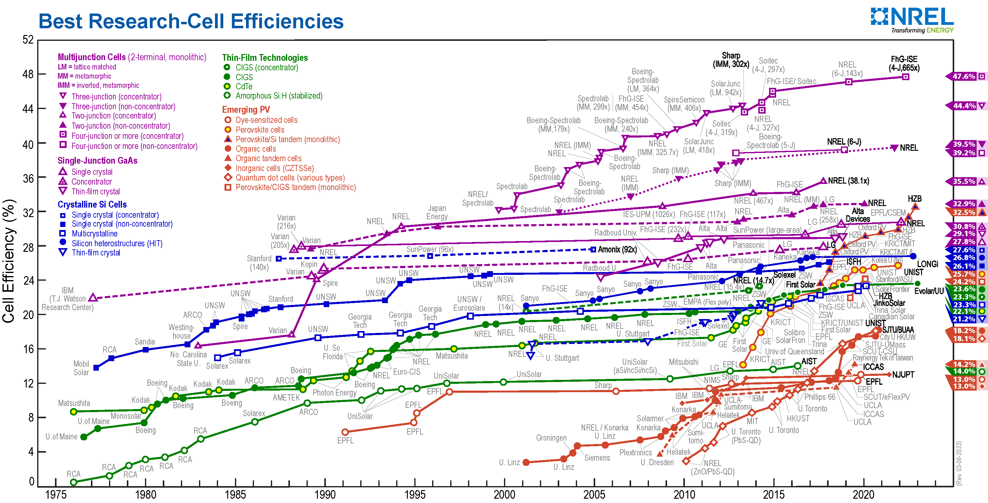 Figure 3.1: NREL Best Research-Cell Efficiencies chart (data through 2022). Public Domain (PD-USGov-DOE), via Wikimedia Commons.
3.3 Temperature: the installer’s recurring antagonist
Heat hurts PV. As a cell warms, its voltage falls (and output power with it). This is not a minor effect. It drives the string-sizing math in Chapter 15 and explains why a hot summer roof can underperform a cold sunny day. Conversely, cold raises voltage, which is the dangerous case for equipment limits. Hold this thought; it becomes a hard design constraint later. Every module datasheet quantifies it with temperature coefficients (Chapter 4).
3.4 The major cell technologies
- Monocrystalline silicon: cut from a single silicon crystal; highest common efficiencies, uniform black appearance, the current mainstream.
- Polycrystalline (multicrystalline) silicon: cast from multiple crystals; slightly lower efficiency and a bluish, flecked look; largely displaced by mono as mono costs fell.
- Thin-film (e.g., CdTe, CIGS, amorphous silicon): deposited in thin layers; lower efficiency per area but good temperature behavior, low-light performance, and a major presence in utility-scale (notably CdTe).
Within crystalline silicon, cell architectures keep advancing. PERC gave way to TOPCon and heterojunction (HJT), each squeezing out more efficiency and better temperature behavior.
Bifacial cells capture reflected light on the back side for a yield bonus on suitable sites.
You don’t need to be a device physicist to install well. You do need to know that technology choice changes the datasheet numbers (efficiency, temperature coefficients, low-light behavior) that drive your design.
3.5 The p-n junction at work
        sunlight (photons)
        │   │   │   │
        ▼   ▼   ▼   ▼
   ┌─────────────────────┐  ← front contact (grid fingers)
   │   n-type silicon    │     extra electrons (−)
   │~~~~~~~~~~~~~~~~~~~~~~│  ← p-n junction: built-in field
   │   p-type silicon    │     "holes" (+)
   └─────────────────────┘  ← back contact
        │             │
        └──[ load ]───┘   electrons flow out the front,
            (DC current)  through the load, back to the rear
A photon frees an electron-hole pair; the junction’s built-in field pushes electrons toward the front contact and holes toward the back, so connecting a load lets electrons do work on their way around. Sun in, DC out.
3.6 Cell technology at a glance
| Technology | Type | Module efficiency | Temp. coeff. (Pmax) | Annual degradation | Position (2026) |
|---|---|---|---|---|---|
| PERC | p-type Si | ~20–21.5% | ~−0.35%/°C | ~0.5%/yr | Budget; being displaced |
| TOPCon | n-type Si | ~22–24% | ~−0.30%/°C | ~0.4%/yr | Mainstream default |
| HJT | n-type Si | ~24–26% | ~−0.25%/°C | ~0.25–0.30%/yr | Premium / high-heat |
| Thin-film (CdTe) | n/a | lower /area | very low | low | Utility-scale niche |
The pattern: moving down the list buys better efficiency, less voltage swing with temperature (gentler string-sizing math, Ch 15), and slower aging, at a higher price. This is why “which module?” is a design decision, not just a price decision.
3.7 Worked example
Example 3.A (why the temp coefficient matters): Two modules both rated 400 W. Module A (PERC) has γ = −0.35%/°C; Module B (HJT) has γ = −0.25%/°C. On a hot roof where the cell reaches 65 °C (40 °C above STC), each loses power:
- Module A: 40 × 0.35% = 14% loss → ~344 W
- Module B: 40 × 0.25% = 10% loss → ~360 W Same nameplate, but Module B delivers ~16 W (≈5%) more in real heat. Over a hot-climate array of hundreds of modules, that gap is real money. It is invisible if you shop on STC watts alone.
Chapter 3 summary
A solar cell is a doped-silicon p-n junction: photons free electron-hole pairs, the junction’s field separates them, and the result is DC current. The band gap sets which photons are usable and caps single-junction efficiency. Heat lowers voltage and output, a fact that becomes a hard design limit. Mono-silicon dominates; thin-film holds utility-scale niches; TOPCon/HJT/bifacial are where the mainstream is moving.
- p-n junction: the field-forming boundary between n-type and p-type silicon; separates photo-generated charges to produce current.
- Band gap: the energy threshold a photon must exceed to free an electron; ~1.1 eV for silicon.
- Electron-hole pair: a freed electron and its vacancy, produced when a photon is absorbed; the raw material of PV current.
- Shockley-Queisser limit: the ~33.7% theoretical efficiency ceiling for a single-junction solar cell.
- Temperature coefficient (γ): the %/°C change in module output power with temperature deviation from STC.
- STC (Standard Test Conditions): the 1,000 W/m², 25 °C, AM 1.5 reference conditions used for module power ratings.
- PERC: passivated-emitter-and-rear-cell p-type silicon; the previous mainstream standard.
- TOPCon: tunnel-oxide-passivated-contact n-type silicon; current mainstream default.
- HJT (Heterojunction Technology): n-type silicon with amorphous silicon layers; best temperature coefficient and lowest degradation of commercial silicon cells.
- Bifacial: a cell/module design that captures light on both front and rear surfaces.
Full definitions: Appendix A (glossary).
Practice Problems: Chapter 3
- In one sentence, what does the p-n junction’s built-in field actually do for the cell?
- Why do photons with energy below the band gap contribute nothing?
- A module has γ(Pmax) = −0.30%/°C. Its cell runs 35 °C above STC. What percentage of rated power is lost to temperature?
- Two 410 W modules differ only in temperature coefficient (−0.34 vs −0.26%/°C). At 30 °C above STC, how many watts does each produce, and what’s the difference?
- Why is the Shockley-Queisser limit not a barrier for tandem cells?
- A buyer picks the cheapest module by $/W for a hot desert install. What design risk have they likely ignored?
Solutions: Chapter 3
- It separates photo-generated electrons and holes before they recombine, creating usable voltage/current.
- They lack the energy to lift an electron across the band gap, so they pass through unabsorbed (as far as power generation goes).
- 35 × 0.30% = 10.5% lost.
- −0.34%: 30 × 0.34% = 10.2% loss → ~368 W. −0.26%: 30 × 0.26% = 7.8% loss → ~378 W. Difference ≈ 10 W per module.
- Tandems stack absorbers with different band gaps, capturing more of the spectrum than any single junction can, so the single-junction ceiling doesn’t apply.
- The cheapest module likely has a worse temperature coefficient, so it sheds more output in desert heat. The lowest $/W at STC can be the worst value in the field.